
Table of Contents
Agilent / Keysight U1273A Display Interface Adapter
Introduction
I was an early adopter of the (back then) Agilent OLED multimeters and have owned a U1273A for many years now. It didn't see too much use recently, so I was mortified to find the display had spontaneously died on my unit. Well, not exactly died, but gotten so dim that it could only be read in complete darkness. It seems to be a reasonably common problem with these and similar meters, and there are plenty of stories on the internet of people having similar problems.
Doing a tiny bit of research, the good news is that the display is reasonably standard (in terms of size and interface), and easily replaced. The bad news is that the controller used on the display is obsolete, and modern displays tend to use different controllers. Whilst they are largely backwards-compatible as far as the interface and protocol are concerned, there are some differences in the mapping of the display that prevent them from being used as a drop-in replacement.

Original
The following describes my approach of making a modern display usable in the U1273A multimeter. All the design files and some notes regarding building your own adapter can be found towards the bottom of the article.

Copy
Issues
The controller on the original display is a SSD1303. Whilst newer controllers (e.g. SSD1309) are largely backwards-compatible as far as the command set is concerned, the display memory mapping in different.
Level 1: Column direction
This is a relatively basic issue, and is actually one where others have already developed solutions for. It's also not so much an issue of the display controller as such, but more to do with how the display manufacturers conventionally map the physical display to the controller outputs. In short, most displays with a SSD1309 controller seem to have column 0 of the display memory mapped to the right-hand edge of the display, whereas the original display of the U1273A has column 0 mapped to the left-hand edge of the display.
This means that if a SSD1309 display is used, the image will be mirrored on the display. satanistik on the EEVblog forums found a very simple solution for this issue (which was the motivation to start this project), namely to have a tiny bit of discrete logic that flips a bit in a command telling the display to scan the columns in the opposite direction, thus un-mirroring the image.
Whilst this fix does make the display readable and has been successfully used by many people, it does leave some artifacts on the display, which I found not acceptable.
Un-mirrored display. Note the horizontal shift and artifacts in the last 8 rows
Level 2: Display memory
The SSD1303 controller's display memory is actually 132 columns wide, with only 128 visible (see illustration below). To make matters more complicated, the visible area in the original display starts with column 2, which means that if a SSD1309 display (with only 128 columns of display memory, all of which are visible) is used, the contents are offset by two columns and then wrap around the right-hand edge of the display.

Mapping of video memory to pixels between SSD1303 and SSD1309
The solution to that is to intercept all addressing commands to the display, and subtract two from the column address, which means that all display contents are displayed correctly within the visible 128 columns.
However, there is a further complication in that the multimeter actually does write to the first two (invisible)columns as well. I noticed that for the minus sign, which is written starting from column 0. With the simple “subtract 2 from all addresses” approach, this means that the beginning of the minus sign would then wrap around and start at column 126. Therefore, it is also necessary to suppress any writes to columns 0 and 1, and shift subsequent writes accordingly so that they are positioned correctly.
Level 3: Bottom Rows
A final issue I noticed were artifacts in the bottom few rows of the display. Whilst I am not 100% sure what is happening exactly and whether this is the same across firmware versions, the following is how I understood (and worked around) the problem: After initialising the display, the multimeter seems to read a number of bytes from the display memory of the last 8 rows (starting at column 497(!) for no apparent reason). As the display memory should be initialised to all 00 (pixels cleared), all of these read operations should return return 00. The multimeter then writes back a number of bytes to the last 8 rows - which consist of the data it just previously read in the regions that will be overwritten by the indicators (e.g. auto power off, auto-range, etc), plus pixels cleared in the regions in between.
There are two issues coming from this behaviour: First, neither the previously developed technique for un-mirroring the display, nor mine support reading from the display (although I could implement reading with not too much hassle in the FPGA). Therefore, the multimeter doesn't necessarily read back 00, but whatever state the bus lines are at when they are not being driven - which in my case was FF due to the pull-ups on the FPGA inputs.
The second issue is that the multimeter writes back the read data to the display, starting at an address that that requires multiple wrap-arounds. Therefore, the read pixels (which are not 00 as they were supposed to) will end up in locations where they will never be overwritten by the indicators, therefore creating artifacts on the screen.
The “correct” solution would obviously be to let the multimeter read back the display memory and then adjust the writes again to correctly map them to the visible area of the display. However, it doesn't seem like the multimeter does anything with the data it reads back, or that there is any benefit to initialising the bottom few rows with anything but 00, and therefore I decided to simply intercept that particular write command and substitute whatever data the multimeter is sending with 00.
In addressing the above three issues, I think I managed to get to a place where a SSD1309 display can be used in the U1273A giving the same visual appearance as the original display. Of course, if you are aware of any other details that I haven't come across yet or different behaviour in newer firmware versions, please let me know.

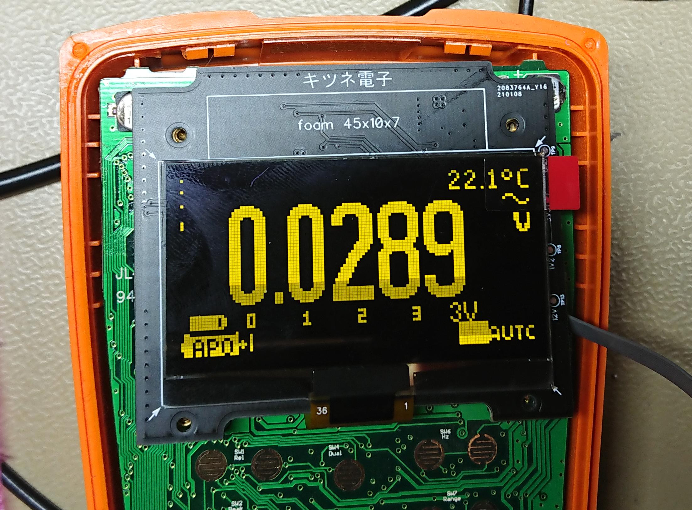
SSD1309 display in U1273A
Implementation
I decided that probably the easiest approach would be to replace the entire display carrier board and replicate its functionality (power supplies for the display) and add the protocol translator onto it. The following figure shows a block diagram of the board.

Block diagram
There is nothing particularly unusual or technically challenging, so I will just outline some of the major design points and only go into details that I found interesting.
Choice of FPGA
Obviously the biggest decision was how to implement the required functionality. Whilst technically it would have been possible to do it with some discrete logic, this seemed a bit silly and would not have allowed for any flexibility. Therefore, the question was mosty between a microcontroller and programmable logic.
Initially, I was tending towards a microcontroller. Even a simple AVR running at a sensible clock speed should be able to (just about) handle data from the parallel interface. However, I was a little bit concerned about power consumption, as the microcontroller would have had to run flat out for most of the time. Upon reflection, I don't think it would have been that big an issue, and it certainly would have resulted in simpler hardware.
After much searching, I decided on a small FPGA to do the job, in particular an ICE5LP1K. The nice thing about an FPGA is that (for this particular part), the static power consumption is close to zero, and the logic only needs to be clocked with the data, resulting in very low overall power consumption. There are obviously some downsides to using an FPGA compared to a microcontroller, in particular, the supporting hardware is more complex (power supplies).
It is also worth noting that the ICE5LP1K has non-volatile one-time programmable internal configuration memory, which eliminates the need for an external configuration flash. However, for development and flexibility later on, I still put down an external configuration flash on the board. With an external flash, the time to configure the FPGA after power-up is a little bit slower, but still plenty quick enough to be ready before the multimeter starts configuring the display.
Power Supplies
I did try to put some effort into the architecture and supply of the power supplies for two reasons: First, I really wanted the whole board to be as low power as possible, and secondly, I also wanted to do my best to try and meet the FPGA's power supply specifications. Whilst I don't think the latter is really too critical, seeing that many of the reference circuits don't seem to care too much, I still thought it would be a good exercise and if nothing else, should make the design just a little bit more robust.
This really boiled down to searching parts with the appropriate specification - i.e. low quiescent currents, high efficiency, appropriate slew rates, etc.
In the end, the power consumption of the FGPA (with the interfaces running) and its supplies is 750uA, which I find is very acceptable.

Power-up timing
The turn-on behaviour is almost what I had hoped for - the sequencing of the power supplies and timing of the reset is all within specification, however, the ramp time of the 1.2V power supply is a little bit on the fast side (16.6V/ms). This is just outside the specifications in the datasheet (0.6V/ms - 10V/ms), but I really don't think it's that critical, and so I will just leave this as it is unless it turns out to be a problem. The 3.3V supply is well within spec (2.69V/ms). The graph also shows very nicely that the configuration of the FPGA finishes in just under 20ms after reset is de-asserted, leaving around 80ms before the multimeter starts talking to the display in earnest.
Construction
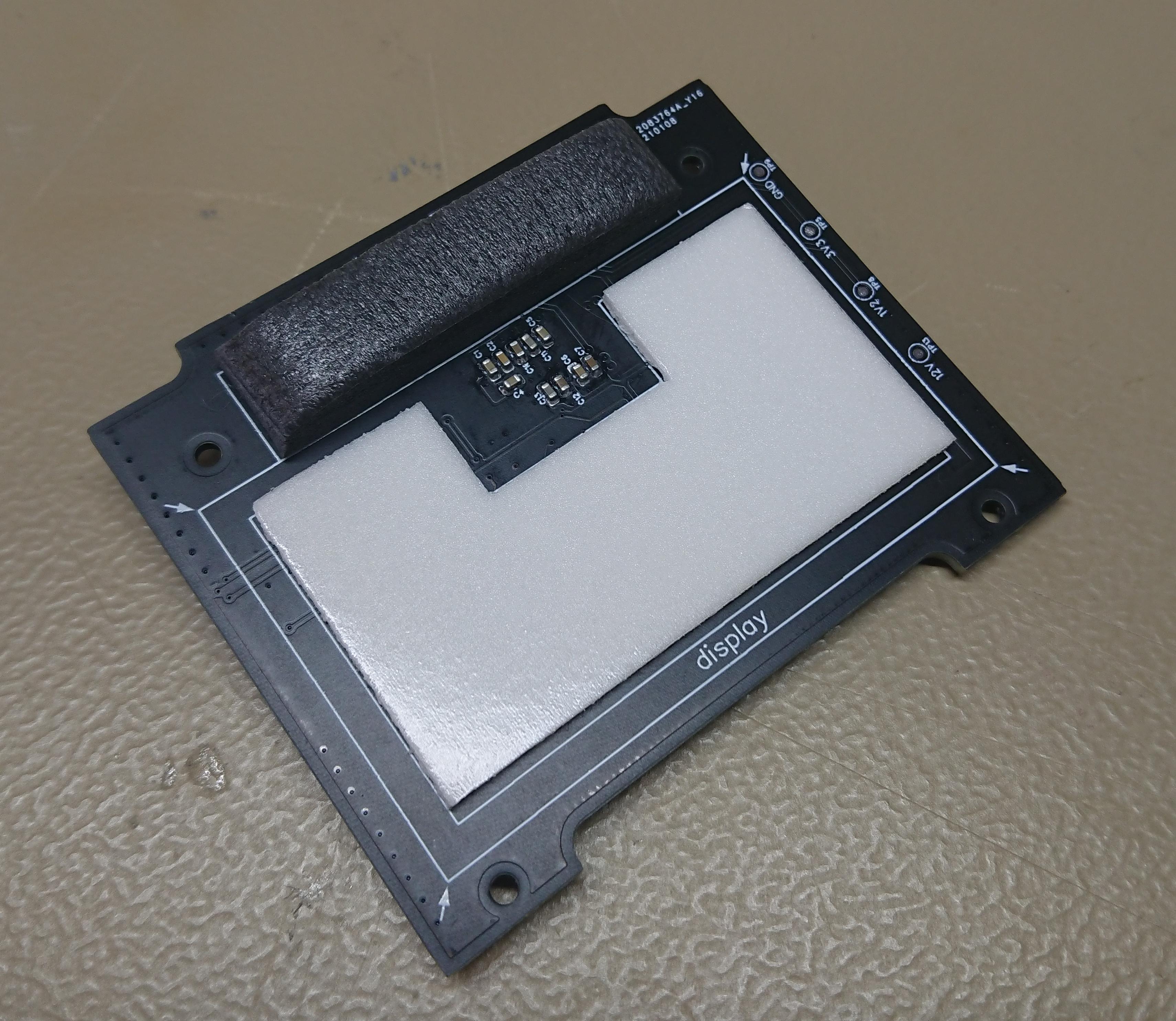
The mechanical construction is (hopefully) a faithful copy of the original board and it should fit with no real issues. There are a few mechanical dimensions where I am not 100% confident (e.g. I swear that the left and right mounting holes are offset by 0.1mm on the original board), but overall nothing that should be of too much concern. There are two bits of foam (one single-sided adhesive above the display, one double-sided adhesive between the display and the PCB) that will need cutting to size and sticking onto the board, but aside from that there is nothing really noteworthy about the mechanical assembly.
Before mounting the display
Choice of Display Interface
One quick note on the display connector: I have chosen to use a ZIF connector for the display, rather than the soldered display of the original module. While the connector will add slightly to the BOM cost, I felt that being able to easily replace the display (in case of any any accidents) was worth it. Also, for one-off hand assembly, I think plugging a flex into a ZIF connector is just a lot less hassle and bears less risk of breaking the display during the assembly process.
Design Files and Notes
If you would like to build your own interface adapter board, you can find the design files below:
- Schematic PDF display-if_r0_schematic.pdf
- Assembly drawings PDF display-if_r0_assembly.pdf
- Design files (DipTrace 4.0) display-if_r0_diptrace.zip
- Gerber files display-if_r0_gerbers.zip
- Bill of materials display-if_r0_bom.csv
- HDL (Verilog source, iCEcube project, constraints file, HEX file) display-if_hdl_v0.1.zip
(hardware release 0, HDL version 0.1)
Notes on Hardware
I did not encounter any particular issues assembling the board and it should work straight away if built according to the design files.
The board is a 4-layer design, intended to be made to 1.6mm final thickness. There are some fairly small vias in the design (0.2mm hole / 0.15mm annular ring), but nothing too challenging. It's all within JLCPCB's standard capabilities and I had no issues with the boards made by them.

View of of underside
Notes on HDL / FPGA programming
I have included the iCEcube2 project file and preserved the directory structure, but for some reason it doesn't seem to pick up the pin constraints file, so you'll have to add that manually (displayif_Implmnt/sbt/constraint/displayif_pcf_sbt.pcf). It might also be a good idea to just check the device settings have been read correctly, in particular that the Internal Oscillator Frequency is set to medium or high (the default of “low” means reading the configuration flash might take too long).
There is also a very crude testbench included, however, I suspect it is going to be of very limited use.
If you don't care about tinkering with the HDL, just program the hex file (displayif_Implmnt\sbt\outputs\bitmap\displayif_bitmap_int.hex) to the configuration flash. You do not necessarily need a Lattice programmer for this, anything that will program a serial flash through SPI will do (e.g. XGecu TL866II Plus). “displayif_bitmap_int.hex” is the standard Intel Hex file that should work with most programmers. Make sure to keep the FPGA in reset while programming the serial flash.
The HDL was developed and debugged using my multimeter which runs v1.95 firmware. If you are successful in getting it to work on a multimeter with different firmware (or have issues), please let me know and I will add the information.
Display
The design includes a 31pin ZIF connector for the display, which should allow a reasonable range of displays to be used. I have used a Raystar REX012864GYPP3N00000, but I suspect e.g. Vishay OLED-128O064A-LNP3N00000 and similar ones will also work. If you use a different display and found it either works or doesn't work, please let me know and I'll add this information here.
Cost
The component BOM cost comes in at just over €10 at one-off quantities, plus PCB and display, which means you should be able to get a working replacement display for somewhere between €35-€40.
Closing Comments
Future Developments
Since the current design seems to be doing what it needs to do, I don't have any particular intentions of making any changes or developing it further unless I come across something. However, there are some points in the back of my mind which I might want to revisit at some point in the future:
- As pointed out above, I think there is probably more complexity in the power supply circuitry than really necessary. For example, given the low power draw of the FPGA, I think the buck converter could be replaced with a LDO, and the reset generator replaced by a simple RC to shave some cost off the BOM
- Likewise, at the moment a large chunk of the BOM cost is actually in the connectors. I'm sure that with some diligent search for chaper alternatives, this could be reduced somewhat. I also think that the programming connector could be replaced with a Tag-Connect, removing that BOM item entirely. However, for development it was just useful to have a “real” connector.
- It would be nice to have support for different display interfaces. I had actually planned to also put down a footprint for a soldered display, but then ran into the pin number limit of the free version of DipTrace. But something along those lines might make the board more widely applicable.
- also briefly played with the idea of extending the functionality to e.g. also support LC displays. This would not only require probably a little bit more effort on the protocol translation side, but also some extra fun like e.g. using the brightness commands to control the current through the backlight. But that seems like something not really worth the effort.
Similar Efforts
As I said initially, the issue of replacing old SSD1303 displays is fairly widespread - not just our beloved Agilent multimeters, but also coffee machines and other such things. Therefore, other people have also made efforts that allow SSD1309 displays to be used. For example, LCD-store sells a replacement OLED module for €71 (ex VAT), which also utilises a FPGA to do some protocol translation. Judging from their adapter board for the U1253A multimeter, it looks like they are using a Lattice MaxhXO2-256HC FPGA, which needs a lot less support circuitry, but will be a bit worse in terms of power consumption.

IT LIVES!